Materials researchers at North Carolina State University have developed a technique that allows them to pattern graphene, graphene oxide (GO) and reduced graphene oxide (rGO) onto silicon wafers at room temperature by using nanosecond pulsed laser annealing. This technique has led to the formation of atomically-sharp p-n junctions between amorphous carbon and rGO. The researchers are already planning to use the technique to create ultrathin CMOS sensors and DRAM devices.
In the new technique, researchers start with silicon wafers. They top them with a layer of amorphous carbon. Then, the researchers melt the amorphous carbon with a single nanosecond laser pulse, which regrows as graphene. As heat flow is spatially and temporally confined, this technique is ideal for melt processing of carbon, which is susceptible to sublimation.
If the process is done in a vacuum, the carbon forms on the surface as graphene; if it is done in oxygen, it forms GO; and if done in a humid atmosphere followed by a vacuum, it forms heavily reduced GO.
“The current equilibrium processing faces fundamental challenges as the free energy of materials remains unchanged with the number of layers. Using this nonequilibrium technique we can control whether the carbon forms one or two monolayers on the surface of the material by manipulating the intensity of the laser and the depth of the carbon melt.,” says Jay Narayan, the John C. Fan Distinguished Chair Professor of Materials Science and Engineering at NC State and corresponding author of the paper describing this work.
“Our earlier work was on conversion of carbon thin films into diamond or Q-carbon harnessing the superundercooled carbon melt. We have now lowered the undercooling to directly form the thermodynamically stable phase of graphene and control its layer thickness utilizing this process, which can easily be scaled up,” Narayan says. “Using this laser annealing process we can control the melt lifetime, thereby regulating the extent of reduction of GO. To make this rGO film using equilibrium route, the GO films have to be processed at over 2000 K for hours. Our processing is done at room temperature, which significantly drives down the cost.”
“The graphene devices are operational at room temperature with charge carrier concentration of −1.2 × 10²¹/cm3 and localization length of 3 nm. The p–n junction heterojunction diodes have a turn-on voltage of 0.3 V, rectification ratio of 110@±1.5 V, and activation energy of 0.13 eV under reverse bias.” We now have scaled-up the process significantly and electron mobility has been tuned to reach above 200 cm2/Vs,” says Narayan.
“This nanosecond laser processing makes the post-processing of device architectures possible, as diodes can now be fabricated at room-temperature, keeping rest of the wafer at near-ambient conditions”, says Siddharth Gupta, first author of the paper and Ph.D. student at NC State.
What comes now? “Graphene is an excellent conductor, but it cannot be used as a semiconductor. However, rGO is a semiconductor material, which can be used to make electronic devices such as integrated smart sensors and optic-electronic devices. We are working on using this technique to develop smart CMOS sensors and to develop memory devices for computer chips.” Narayan says.
The paper, “Reduced Graphene Oxide/Amorphous Carbon P−N Junctions: Nanosecond Laser Patterning,” was published June. 11 in the ACS Applied Materials and Interfaces Journal under organic electronic devices section. (DOI: 10.1021/acsami.9b05374) Lead author of the paper is Siddharth Gupta, a Ph.D. student at NC State. The work was supported by the Army Research Office grant no. W911NF-17-1-0596.
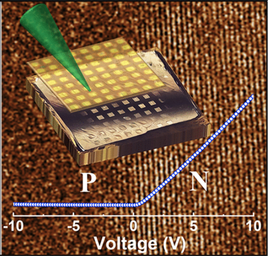
High-resolution transmission electron microscopy image revealing the atomically-sharp interface between heavily reduced graphene oxide and amorphous carbon. The figure also reveals the PN junction IV characteristics acquired at room-temperature. The sketch at top shows the numerous PN junction diodes formed on silicon using a shadow mask to perform nanosecond laser patterning.